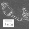
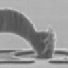
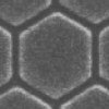
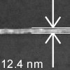
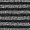
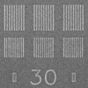
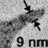
NPGS Sample Pictures
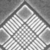
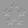
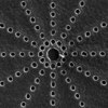
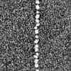
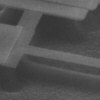
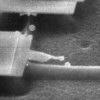
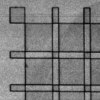
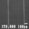
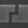
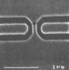
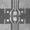
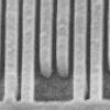
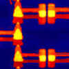
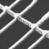

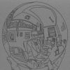
While the images shown above demonstrate very good results in the wide range of applications that NPGS has been used for, when first learning to do lithography, it can be more important to know the cause of common problems. Consequently, the following images are shown to help new users diagnose common exposure problems. By clicking an image below, you will obtain a discussion of the problem displayed and/or instructions on the recommended approach for doing SEM lithography.
Also see the general SEM Optimization Guide and the SEM Lithography Setup Guide.
|
|
|
|
|
|
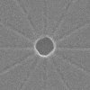
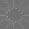
| Gold Standard * |
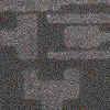
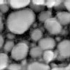
Contamination Spots |
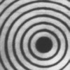
Charging #1 during imaging |
Charging #2 during writing |
Lift-Off* |
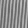
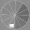
Line Frequency Noise |
|
|
|
|
|
|
|
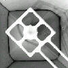
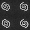
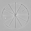
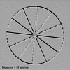
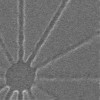
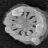
Wheel #1 ~20 nm lines |
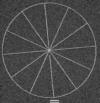
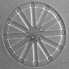
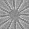
Wheel #2* | Wheel #3* |
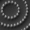
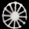
Wheel #4 AFM Image |
Wheel #5 AFM Image |
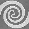
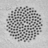
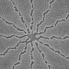
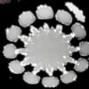
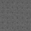
Wheel #6 |
|
|
|
|
|
|
|
Bad Magnification |
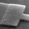
Bad Coating |
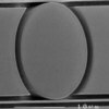
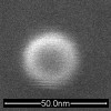
Small Dots |
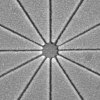
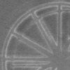
10 kV Wheel |
Negative PMMA |
Double Exposure |
* Image was acquired using the NPGS Digital Imaging Feature.
All images on this site are Copyright (c) by JC Nabity Lithography Systems unless otherwise noted. Permission to display these images for non-commercial uses will be given if a request is made in writing before such use and if proper reference to JC Nabity Lithography Systems is displayed with the image(s).