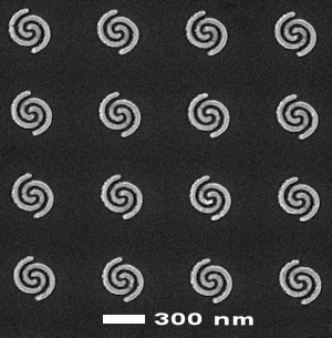
The linewidths of the spirals are quite uniform at ~40 nm.
While this image looks like it could be the result of a typical evaporation and liftoff, the processing steps are quite different:
1) Expose and develop PMMA (as shown below) on Si substrate..
2) Using the PMMA as an etch mask, etch ~40 nm into the Si substrate.
3) Remove the PMMA and evaporate ~100 nm of aluminum onto the etched Si surface.
4) Strip off the thin patterned aluminum film using epoxy and a second substrate.
5) The image above is looking down onto the aluminum film which is now epoxied to a different substrate. The spirals are raised ~40 nm above the background which was the depth of the etch.
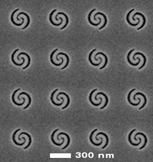
Note how the linewidths appear narrower at the ends and especially near the center of each double spiral. This is a common effect which results when the resist shifts either before or during the imaging. The image of a similar finished device above shows that the linewidths were actually quite uniform after the development.